How To Assembly Printed Circuit Board In House ?
November 17, 2015There are a lot of benefits of the Inhouse make, such like low production costs, fast work cycles that speed the time to market, safety and environmental protection. But How to assembly an Inhouse PCB board? We are about to take the samples from NexPCB factory to show the whole Inhouse making processes.
1. Prepare tools and materials
1)Printed circuit boards, Stencil, Fixation, Reflower
2)Solder paste, Scraper
3)Tweezers, Solder wire, Electric iron


2. Printing of solder paste
The quality of the PCB is great impacted by the quality of solder paste printing. According to the industry analyst, about 60 percent of the rework board due to the poor printing, this causes our more attention in this process. Three basic steps of printing as following:
1)Fix the stencil in the fixation, place the board under the stencil and align the holes.
2)Scrape the solder paste from the front backwards evenly, the angle of scraper to 45-60 degree is appropriate, then put back the excess paste in the front of stencil.
3)Lift the stencil and remove the board with solder paste carefully, a good print is the final result.


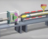
3. Reflower and reflow profile
A correct temperature curve will ensure high-quality soldering joint points. To get a good quality solder point in the PCB assembly, an optimized reflow profile is one of the most important factors.

Table1 Typical PCB reflow temperature setting

Table2 The temperature profile


4. Manual soldering
After preparing the materials of board and components, the tools of flux, solder wire and electric iron, then we get started. But four points should be noted during the soldering:
1)Components for each place should be ready ahead, identify the labels and put them in the neared placement.
2)Wearing a pair of antistatic gloves when soldering, don’t touch the PCB pad and fillets directly.
3)To prevent to soldering scorch, the adjacent components can not be soldered at the same time.
4)Control of soldering temperature, for lower temperature will cause false soldering and high temperature will destroy the components, 200-300 degree will be appropriate.


5. Board test
when all the steps are completed, we have to test the finished board. The test includes appearance test and function test.


To produce a neat and qualified PCB is far more complicated than we described here, it has to go through many more fine processes. The prototyping service of NexPCB factory would be fully meet your custom.
You can also visit our website www.nexpcb.com, to view the specific service information. Here introduce you two boards from NexPCB factory.