News — Design
-
 June 10, 2015
PCB Routing Requirements
When the packing density is permissible, choosing a lower-density routing design to improve reliability and defect-free manufacturing capacity. -
 June 08, 2015
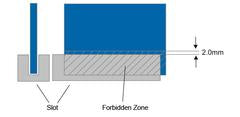
Design of Hole
The design of through hole needs to meet the requirement that the hole diameter to the panel thickness ratio should be greater than 1/6. -
 April 05, 2015
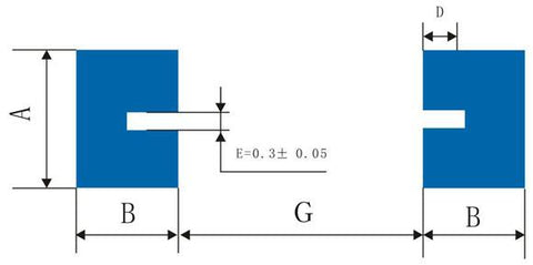
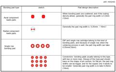
Bonding Pad Design Ⅱ
Cylindrical component bonding pad design - The shape of bonding pad is rectangle. When the reflow soldering process is applied, a concave groove must be designed -
 April 04, 2015
Bonding Pad Design Ⅰ
Cylindrical component bonding pad design - The shape of bonding pad is rectangle. When the reflow soldering process is applied, a concave groove must be designed -
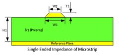 April 02, 2015
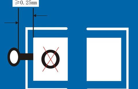
Trance Impedance
Care should be taken to distinguish between single ended and differential trace impedance. High speed single ended signals need to be routed with the specified single ended impedance.


