NexPCB supply a professional design service to the electronics industry. We are able to draw on years of experience at the forefront of PCB design using the most powerful CAD tools.
Project Information And Requirements:
Please provide the following details to get final quote and start working:- Schematic (PDF,JPEG,GIF or PNG)
- Netlist, Partlist, BOM(Allegro, PADS, Altium, Eagle and other popular PCB Design softwares)
- Number of layers (fixed or preferred)
- Size of PCB; Board outline (DXF or picture); Mounting hole diameters and positions; Component positions;
- Trace width; Clearance; Via size; Ring size
- Datasheet or footprint information for each component is also ideal.
- Your other layout requirements.
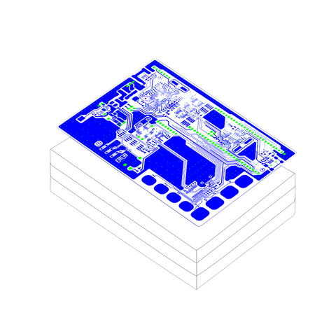
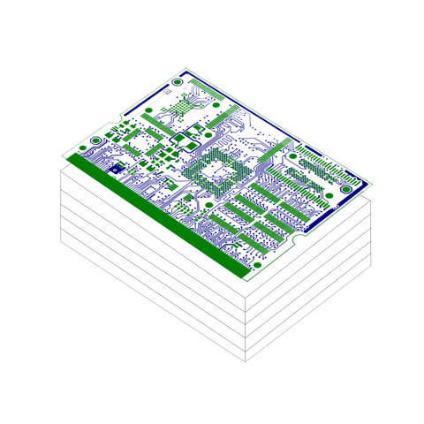
Deliverables:
- PCB.ZIP PCB initial file
- CAM.ZIP Gerber file
- ASM.ZIP Assemble file
- SMD.ZIP Stencil file
- DXF.ZIP Structure file